Connect now
ASIC Solutions

ASIC Design

Developing high quality RTL is challenging because the chip needs to be low on area and power consumption and at the same time provide adequate performance. To overcome this, we leverage dozens of years’ experience of our team and follow stringent design checklist.
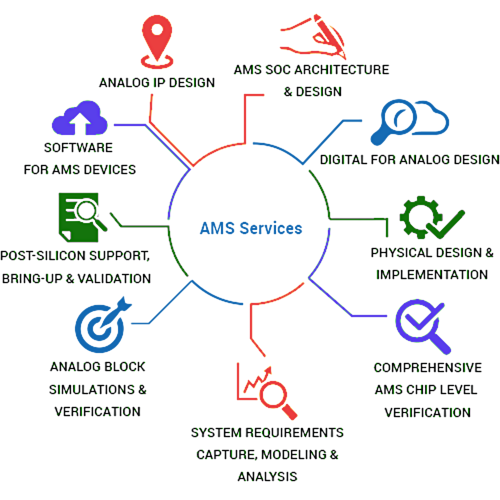
Area Of Expertise

  • Micro-Architecture

  • RTL Development & QC Checks e.g. Lint, CDC

  • Design Timing Constraints

  • Low Power Design Implementation & UPF Checks

  • Logical Equivalance check

  • Synthesis and STA

  • AMBA AXI, AHB, APB, Protocols, OCP, ARM Subsystem

  • Audio, Display, Camera, PCIe, Ethernet, USB Subsystems

  • PCIe, Ethernet, OCP, WLAN, CPU domain

Design Verification

We have the one of the strongest team in DV. Our team can execute verification from scratch of complex SoC’s and IP’s by using latest methodologies such as SV-UVM, UPF and meeting key KPI such as 100% functional and code coverage. We also provide silicon proven VIP for latest IP’s and provide source code and aftersales support to our customers.

  • Advanced IP & SoC Verification

  • SV-UVM Based Constrained - Random Verification

  • Verification Plan, Environment, Test Bench Development

  • Low Power Verification

  • Gate Level simulation

  • Assertion based Formal Verification

  • VIP Development and Integration

  • Palladium, Zebu & Veloce based Validation Silicon validation

  • Methodology

    UVM

    OVM

    RM

    C-based

    System C

    UPF based

    GLS

  • Subsystem

    ARM

    DSP

    Graphics

    Display

    Camera

    Security

    CPU

  • IPs

    PCI-E

    Ethernet

    NVMe

    USB

    MIPI

    DDR

    WLAN

    SDIO

    FlexRay

  • AMS

    Behavioral Modelling

    CO-simulation

    WREAL

    System verification

FPGA based Design

BloomConn team in Emulation and FPGA design have hands-on experience doing the following activities
at several of our clients:

  • ASIC / IP Prototyping with FPGA

  • Processor-based emulation

  • FPGA-to-FPGA, FPGA-to-ASIC, ASIC-to-FPGA conversion

  • Embedded hardware and software support

  • Board design and bring-up

  • System Integration & Validation

Physical Design

We provide support throughout RTL to GDSII stages of ASIC development flow. Our experienced team has developed advanced flows for power aware synthesis (UPF, CPF), timing constraint generation (STA), netlist floor planning for best possible PPA and place and route(PNR) for overcoming ever increasing complexity. Our engineers in-depth knowledge of EDA tools and scripting skills enable us to deliver full turn-key ASIC development.

  • Synthesis

  • STA

  • Floor planning

  • Place & Route

  • Low Power Implementation

  • Crosstalk Analysis

  • All Signoff Checks (PV, STA, IR/EM, LEC etc)

  • ICC2, Innovus, Calibre, RC, DC, RedHawk, PT/PTSI

  • Physical Design

    Block/SoC Level

    Floorplanning

    power Planning/optimization

    Placement & Routing

    Clock Tree Synthesis

    pv – ORC, LVS, ANT, DFM, Density,

    Static and Dynamic EM/IR

    Verification

    Extraction

    ECO Implementation

  • Synthesis / STA

    Synthesis/Formal

    Checking

    Static Timing

    Analysis

    Timing Signoff

    Low power/Multi power Voltage

    Domain Designs

    Crosstalk/Noise/Thermal Analysis

  • Tools

    ICC, ICC2, Innovus, AtopTech, SOC Encounter

    Calibre, ICV, PVS, Assura

    Redhawk, Voltus, Totem Star RC

    Cadence RC, Synopsys DC

    Synopsys PrimeTime/PTSl

    TCL, Shell, Perl scripting

    Varlous Checks/Flow Automation

  • Technology Nodes / Foundry

    10nm (FinFet) & Lower Nodes

    TSMC, UMC, Intel, Samsung

DFT

The BloomConn DFT team has expertise in DFT implementation and DFT verification with all the major industry EDA tools. The team’s expertise is in implementation and verification in the areas of ATPG, BIST and SCAN. The team also has expertise in Test engineering.

Strategies for low test power, low test cost and less test pin utilization, Test pin-muxing, Test clock/Test reset pin identification, planning for on-chip clock insertion.

Strategies for Mixed-Signal DFT, Hard-IP, Analog blocks

User Defined register implementation for all concern control bits. On-chip Clock insertion for respective clock domain, TAP controller and Boundary scan insertion,Test-Pinmuxing

MBIST insertion at block/TOP level, Scan insertion/LBIST insertion, IOwrapper insertion for each DFT blocks, compression/decompression insertion

Expertize in different format of pattern generation i.e. Verilog, ASCII, different ATE format, Cell-aware pattern generation, Power-aware pattern generation, Pattern re-targeting ,Zero-delay as well as timing verification across different SDF corners, ATE pattern generation, and Silicon debug of failing patterns

Expertize in MBIST verification for Block level as well as Full-Chip level, MBIST verification for repairable and nonrepairable memories.

No-timing simulation & debug, timing simulation & debug across different SDF corners, ATE pattern generation for MBIST controllers, Silicon debug of failing patterns

Expertise in BSCAN verification with respect to IEEE 1149.1 & IEE1149.6 protocol

Simulation debug without and with SDF across different PVT corners, ATE patterns generation for different requirements and silicon debug

Expertize in ATE test program development for Digital domain, Analog domain, Mixed signal, RF domain, Program development for engineering evaluation as well as production support

ATE program development and debug support on multiple tester platform, Multi Site program development, program conversion from one platform to another platform, PVT characterization

Expertize in Load boards, Handler Interface Board, DUT Interface Board-TE Expertize in Probe Card, Probe Interface board, Device characterization board, burn-In board Expertize in different kind of BGA, Leadframe, Hermetic package through our partners

RF / Analog

The BloomConn analog team is well versed in analog layout and in AMS modeling and verification. Our Layout expertise includes In-depth expertise on RF, Analog and Power management IPs including PLLs, DC-DC Convertors, DLLs, LDOs, etc in all the leading foundries in all the technology nodes. Our AMS expertise includes both modeling and verification

Analog, RF, Power Management IC, Memory

SerDes, LDO, BGR, DC-DC Converters, Phase Interpolator, ADC, DAC, PLL, Power Regulators, SRAM

Mixed Signal – VHDL, Verilog AMS, WREAL, SystemVerilog Net type

Analog – Verilog A

Expertise in Verilog, VHDL, SV, and UVM

AMS Verification with Models and Digital designs – Digital/Analog Top

Verification with Analog Models and SPICE

SerDes, ADCs, DACs

IC – LDO, Buck/Boost, ChargePump, Fuel Gauges, GPIOs etc

Mixed Signal

Bloomconns offers design services in the Analog domain covering analog design, Layout & verification. The team is proficient in Memory Design, High Speed I/F, IO, Power Management and Library Development. Apart from design, the team is also capable of developing electrical accurate analog models in industry standard languages and enabling a coverage driven verification methodology for verifying these models.

  • Analog IP design

  • Library Development (Std Cell, IO's, and Memories)

  • Standard Cell characterization

  • Test chips

  • AMS Modelling & Verification

  • Process Migration of libraries

Contact Us

Get in touch with us BloomConn