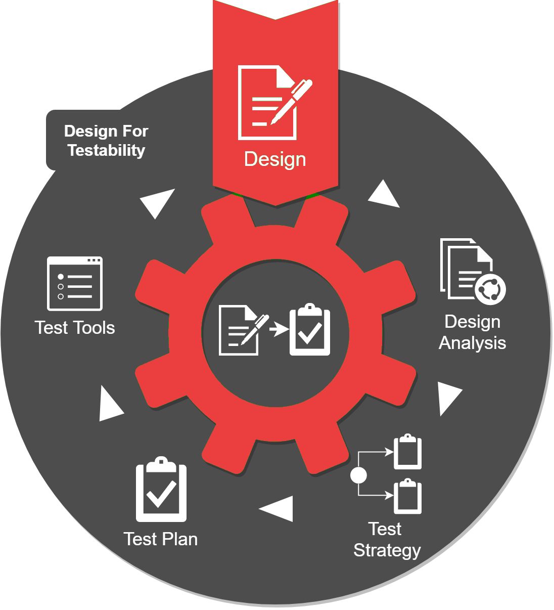
Connect now
Back End Design

Physical Design

We provide support throughout RTL to GDSII stages of ASIC development flow. Our experienced team has developed advanced flows for power aware synthesis (UPF, CPF), timing constraint generation (STA), netlist floor planning for best possible PPA and place and route(PNR) for overcoming ever increasing complexity. Our engineers in-depth knowledge of EDA tools and scripting skills enable us to deliver full turn-key ASIC development.

  • Synthesis

  • STA

  • Floor planning

  • Place & Route

  • Low Power Implementation

  • Crosstalk Analysis

  • All Signoff Checks (PV, STA, IR/EM, LEC etc)

  • ICC2, Innovus, Calibre, RC, DC, RedHawk, PT/PTSI

  • Physical Design

    Block/SoC Level

    Floorplanning

    power Planning/optimization

    Placement & Routing

    Clock Tree Synthesis

    pv – ORC, LVS, ANT, DFM, Density,

    Static and Dynamic EM/IR

    Verification

    Extraction

    ECO Implementation

  • Synthesis / STA

    Synthesis/Formal

    Checking

    Static Timing

    Analysis

    Timing Signoff

    Low power/Multi power Voltage

    Domain Designs

    Crosstalk/Noise/Thermal Analysis

  • Tools

    ICC, ICC2, Innovus, AtopTech, SOC Encounter

    Calibre, ICV, PVS, Assura

    Redhawk, Voltus, Totem Star RC

    Cadence RC, Synopsys DC

    Synopsys PrimeTime/PTSl

    TCL, Shell, Perl scripting

    Varlous Checks/Flow Automation

  • Technology Nodes / Foundry

    10nm (FinFet) & Lower Nodes

    TSMC, UMC, Intel, Samsung

DFT

The BloomConn DFT team has expertise in DFT implementation and DFT verification with all the major industry EDA tools. The team’s expertise is in implementation and verification in the areas of ATPG, BIST and SCAN. The team also has expertise in Test engineering.

Strategies for low test power, low test cost and less test pin utilization, Test pin-muxing, Test clock/Test reset pin identification, planning for on-chip clock insertion.

Strategies for Mixed-Signal DFT, Hard-IP, Analog blocks

User Defined register implementation for all concern control bits. On-chip Clock insertion for respective clock domain, TAP controller and Boundary scan insertion,Test-Pinmuxing

MBIST insertion at block/TOP level, Scan insertion/LBIST insertion, IOwrapper insertion for each DFT blocks, compression/decompression insertion

Expertize in different format of pattern generation i.e. Verilog, ASCII, different ATE format, Cell-aware pattern generation, Power-aware pattern generation, Pattern re-targeting ,Zero-delay as well as timing verification across different SDF corners, ATE pattern generation, and Silicon debug of failing patterns

Expertize in MBIST verification for Block level as well as Full-Chip level, MBIST verification for repairable and nonrepairable memories.

No-timing simulation & debug, timing simulation & debug across different SDF corners, ATE pattern generation for MBIST controllers, Silicon debug of failing patterns

Expertise in BSCAN verification with respect to IEEE 1149.1 & IEE1149.6 protocol

Simulation debug without and with SDF across different PVT corners, ATE patterns generation for different requirements and silicon debug

Expertize in ATE test program development for Digital domain, Analog domain, Mixed signal, RF domain, Program development for engineering evaluation as well as production support

ATE program development and debug support on multiple tester platform, Multi Site program development, program conversion from one platform to another platform, PVT characterization

Expertize in Load boards, Handler Interface Board, DUT Interface Board-TE Expertize in Probe Card, Probe Interface board, Device characterization board, burn-In board Expertize in different kind of BGA, Leadframe, Hermetic package through our partners

Contact Us

Get in touch with us BloomConn